

Features
- FCC approved method of EMI attenuation
- Non-PLL phase controlled Active EMI management architecture
- Generates a 1X low EMI Phase Modulated replication of the input signal.
- Vdd 1.65V – 3.6V. 10 MHz to 54 MHz
- Multiple Deviation Selections
- Minimum frequency deviation selection capability
- Power Down Mode
- 8-pin WDFN package
- Supports automotive reliability standard
Product Description
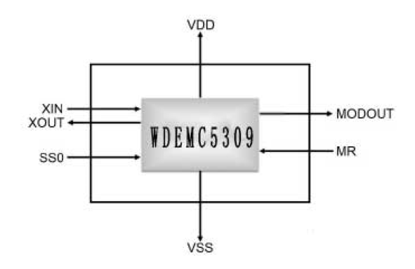
The WDEMC5309 is a versatile 1x Active EMI management IC designed to provide system wide reduction of Electromagnetic Interference (EMI) and Radio Frequency Interference (RFI) from clock and data sources. The WDEMC5309 allows significant system cost savings by reducing the number of circuit board layers, ferrite beads, shielding and other passive components that are traditionally required to pass EMI regulations. The WDEMC5309 family of mobile active EMI management. ICs is unique in it’s design and is based on PulseTake’s
phase controlled Active EMI management technology.
This allows operation on aperiodic as well periodic signals.By the precise placement of the edges of the reconstructed input signal, the peak energy of the output is distributed over a wider and controlled energy band thereby significantly lowering system EMI compared to the typical narrow band signal produced by oscillators and most frequency generators.
The WDEMC5309 has an input frequency range of 10MHZ to 54MHz over a wide voltage range of 1.65V to 3.6V.The device can be placed in a“ nonmodulated clock mode” by setting the SSEN pin to GND where sets the MODOUT pin to no modulated clock output. The device has one “deviation control pins” SS0 to allow flexibility and optimization of both EMI compliance as well as in system design.The device is available in an 8 pin DFN package.
使用方法
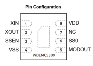
Pin 1 XIN 接时钟输入,主板MCU时钟拆下来安装在此,记得时钟晶体接负载电容
Pin 2 XOUT 接时钟输出,主板MCU时钟拆下来安装在此,记得时钟晶体接负载电容
Pin 3 SSEN 接使能端,滤波功能打开,或者关闭,可通过IO实现软件控制,上拉时的调制滤波后的时钟输出(内部接上拉电阻)。 如果下拉,则无调制滤波时钟输出,接GND后滤波芯片就不工作。意思就是说可以悬空,接地就等于没有接这颗芯片。
Pin 4 VSS 接电源参考地
Pin5 MODOUT 接CLK时钟滤波输出,接主板MCU的CLK时钟输入。
Pin6 SS0 接GND为低电平滤波幅度最大,悬空或者上拉接VCC为高电平滤波功能最小。(注意:如接地或者很小电阻接地,可能时钟输出很弱,那么滤波幅度越大,功能可能丢失。)
Pin7 NC 空脚,悬空不管
Pin8 VDD 接电源2.5V或者3.3V
注意事项:
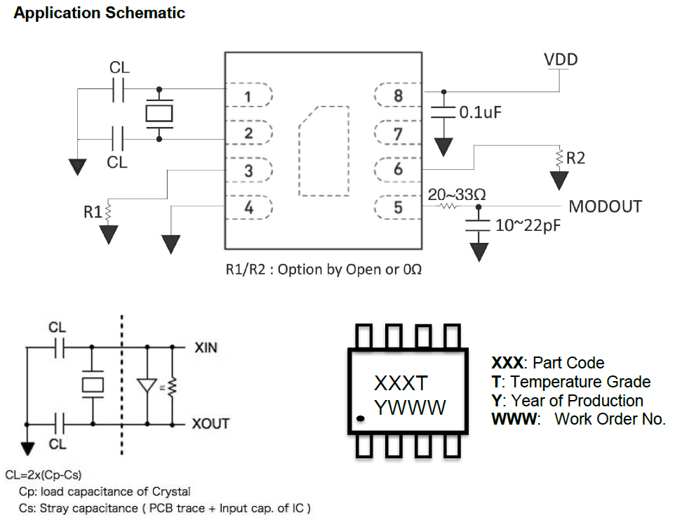
1、Pin1 & Pin2的负载电容的GND必须靠近Pin4 GND。
2、Pin3需悬空才有效果。
3、Pin5上述应用电路10~22pf电容不是必须,但是需要预留,依据实际测试情况酌情添加。(此颗电容必须回路最近WDEMC5309的Pin4)
4、Pin6的接地必须靠近Pin4,可以直接接地,滤波效果应该为最佳,如果机器启动不了,可以把这个电阻适当加大。
5、Pin8的VDD供电建议接Π型滤波,即Cap+Bead+Cap滤波架构。
WDEMC5309规格书下载
更多技术问题,可以联系曾工 139 2899 3907
 扫码技术咨询